Nano-ink tech for bio-inspired electronics, without the cleanroom.
Cutting-edge tools, ink, and software. Backed by the NSF and decades of research.
Trusted By




All-in-One, Configured to Your Process
Five integrated modules share one precision stage. Run them together, or build the system around only the steps your process needs.
Explore the Platform- 1
Precision Gantry
Precise gantry robot carrying every module
3-axis XYZ nm encoder resolution - 2
EHD Printhead
Features down to 1 µm
up to 100 droplets / s - 3
Optical Analysis
Fast surface scanning
under 1 µm resolution - 4
Microtransfer
Transfers patches of printed ink
down to 2×2 µm² ink patches - 5
Spin Coater
Large-area uniformity, automated deposition
down to 200 nm coatings
What it prints
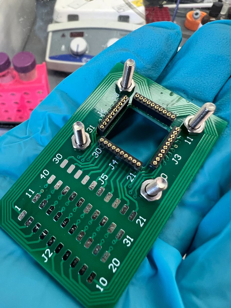
- Resistive switching matrices
- 2D & 3D bioprinting
- Flexible electronics
- And more
Everything You Need for printed electronics
Conductive Ink Formulation
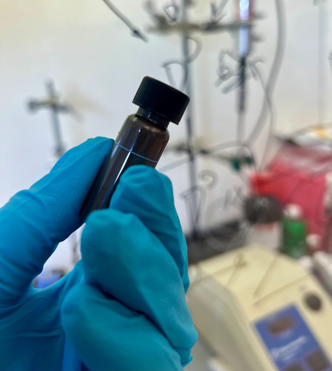
Electroconductive silver and gold nanoparticle inks engineered for printed electronics, from fine-feature inkjet to direct-write deposition.
Explore service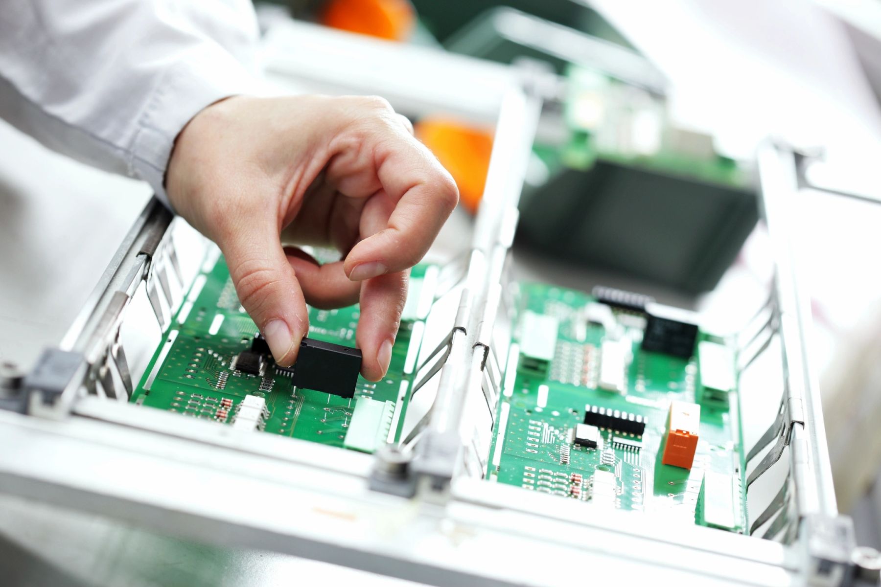
Optical Profilometry
High-resolution surface metrology with confocal, interferometric, and focus-variation modes in a single instrument.
Explore service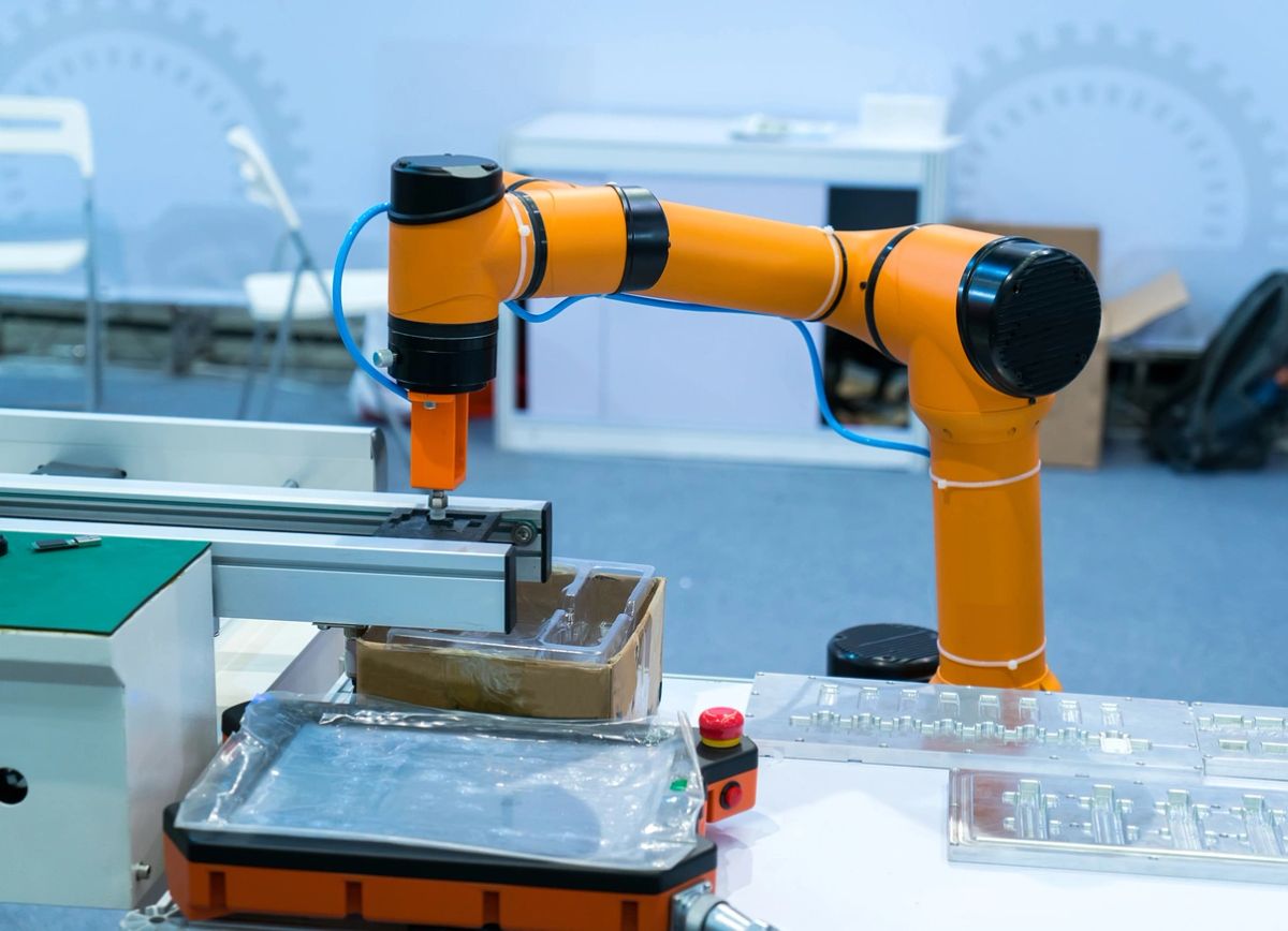
Laser Micromachining
Ultrafast and UV laser processing for precision ablation, drilling, and patterning across metals, ceramics, polymers, and semiconductors.
Explore serviceCharacterize it, Machine it, then Print it in-house .
Neuroink is a nanotechnology company that develops novel nano-ink technology and scalable microprinting for next-generation bio-inspired electronics. We specialize in formulating functional inks and software that enable the production of complex nanocomposites and neuromorphic computation devices without the need for expensive cleanroom lithography.
Nano-Ink Formulation
Functional inks engineered at the nanoparticle level, not adapted from off-the-shelf chemistry.
Scalable Microprinting
Software-driven deposition that scales from a single R&D sample to production volume.
No Cleanroom Required
Complex nanocomposites and neuromorphic devices, without expensive cleanroom lithography.
From First Question to Handoff
Scope the Problem
Walk through the applications assistant or send us a spec, drawing, or sample. We confirm feasibility and the right instrument or process window.
Feasibility & Quote
We run a bounded feasibility pass, such as a scan, a test cut, or a formulation trial, and return data plus a fixed-scope quote or demo proposal.
Execute & Hand Off
We deliver characterization data, machined parts, or ink formulation with full process documentation, ready for your QC or production partner.
Frequently Asked Questions
Why printed electronics?
Printed electronics let us build devices at nearly any size, from microns to meters, far more cheaply than conventional cleanroom lithography, with high scalability at low cost and the freedom to work with unconventional materials like nanowires and nanoplatelets.
Why functional nano-inks?
Functional nano-inks make it easy to tune a pigment's bandgap, deposit on nearly any surface or layer, and support a flexible range of device designs, including novel devices like memristors and quantum Josephson junctions, without cleanroom or lithography equipment.
What surface metrology tolerances can Neuroink characterize?
Our confocal and interferometric systems resolve fine vertical and lateral features, covering roughness, step height, coating thickness, and 3D topography in a single non-contact scan. We'll confirm fit for your specific tolerance in a working session.
Which materials can be laser micromachined?
We routinely process metals, technical ceramics, glass, silicon, polymers, and multilayer stacks. Pulse duration and wavelength are matched to the material's absorption profile to minimize heat-affected zone and recast.
Do you support both prototyping and production volumes?
Yes. Engagements typically start with feasibility and process-window studies on production-representative samples, then transition to pilot runs and, where applicable, scaled deposition or machining protocols for your production partner.
Can conductive ink formulation be paired with profilometry or micromachining?
Frequently. Printed silver and gold traces are profiled for thickness and surface roughness post-cure, and laser structuring is used to define fine-pitch features or trim printed conductors. We scope this as one integrated program when useful.
What do you need from us to scope a project?
A brief description of the part or material, a target specification or failure mode, and a sample or CAD drawing if available. The conversational form below routes this directly to our applications engineering team.
Scope Your Next Project
Answer a few questions and we'll route you to a quote, a live demo, or the right spec sheet. No account, no sales gate.

A structured intake form that routes directly to our applications engineers. No account required.