Print working devices in your own lab, without the cleanroom.
One benchtop platform for teams who need to iterate faster than an outside vendor allows, from first prototype through production volume.
Trusted By



The Problem With Iterating Externally
Iteration Is Slow
Every design change waits on an outside vendor's schedule instead of your own.
Prototype and Production Don't Match
A process that works on the bench doesn't always carry over cleanly to volume.
The Cleanroom Barrier
Traditional lithography puts a facility and a queue between you and your next revision.
All-in-One, Configured to Your Process
Five integrated modules share one precision stage. Run them together, or build the system around only the steps your process needs.
- 1
Precision Gantry
Precise gantry robot carrying every module
3-axis XYZ nm encoder resolution - 2
EHD Printhead
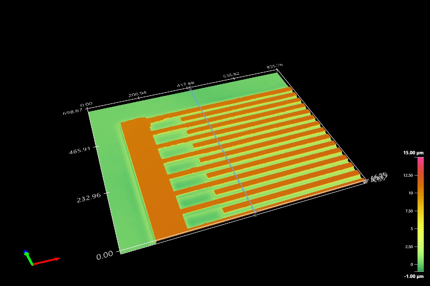
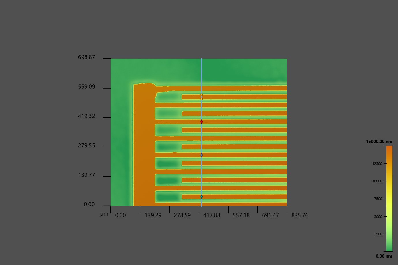
Features down to 1 µm
up to 100 droplets / s - 3
Optical Analysis
Fast surface scanning
under 1 µm resolution - 4
Microtransfer
Transfers patches of printed ink
down to 2×2 µm² ink patches - 5
Spin Coater
Large-area uniformity, automated deposition
down to 200 nm coatings
What it prints
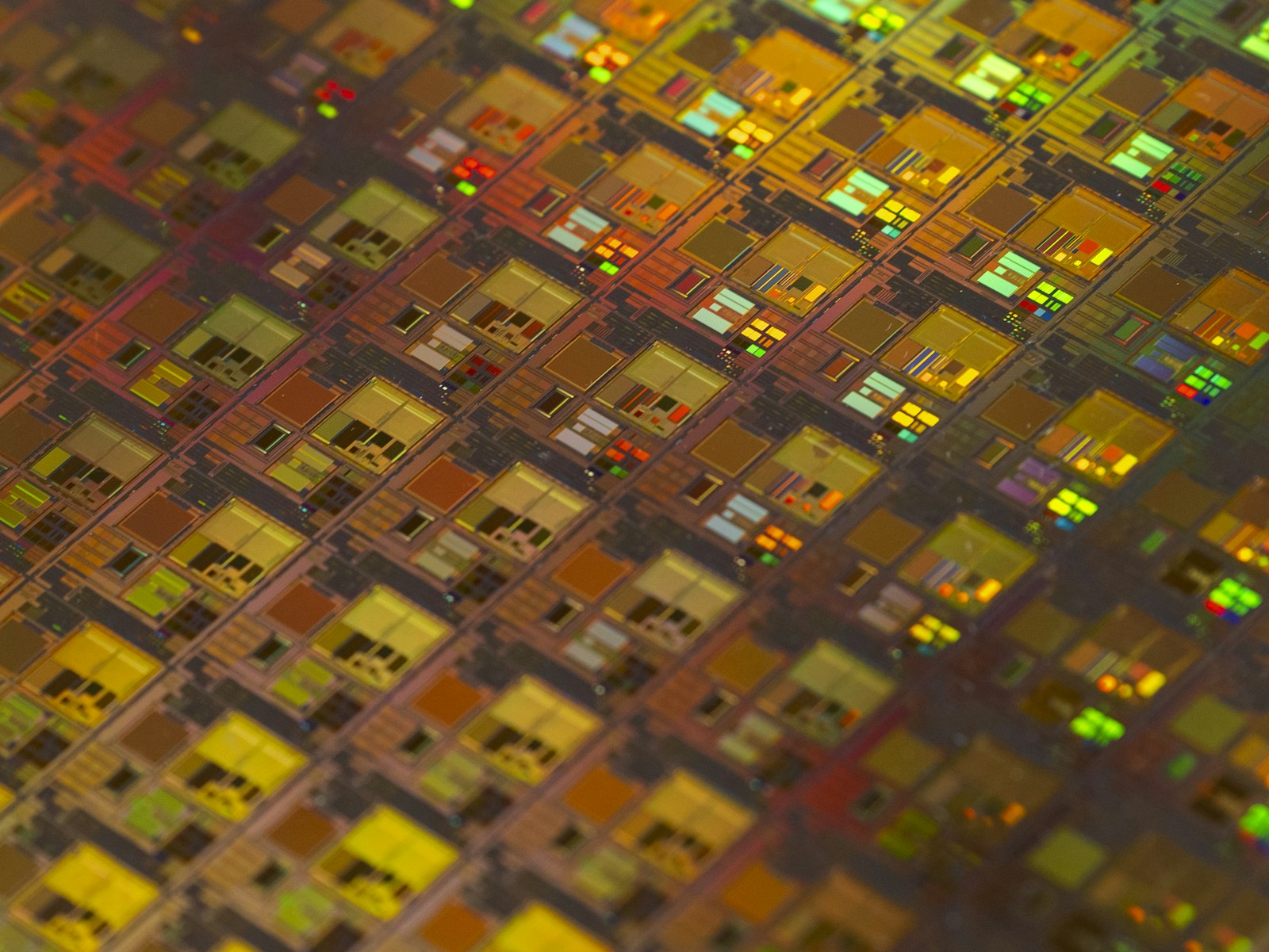
- Resistive switching matrices
- 2D & 3D bioprinting
- Flexible electronics
- And more
From Design to Device, on Your Bench
With printing, inspection, transfer and coating on one instrument, a design moves from first pass to batch without leaving your lab. No lithography equipment, no cleanroom, and no waiting on an outside vendor between revisions.
- Biosensors & Diagnostics
- Microcircuits & Flexible Electronics
- Biological Assays & Lab-on-Chip
- RF & Antenna Structures
Common Questions
What is this platform, in one sentence?
A benchtop microfabrication system that takes a design from early prototype through production volume without cleanroom lithography.
Who is this built for?
R&D and applications teams in defense, university, and commercial device groups who need to iterate on microdevices faster than an outside vendor allows.
Do we need to know exactly what we're building before we talk to you?
No. Bring a rough idea, a sample, or a spec, and we'll help you scope whether and how it fits.
Talk to Applications Engineering
A structured intake form that routes directly to our applications engineers. No account required.