Micron-Scale Precision, Matched to Your Material
Ultrafast and UV laser processing for micron-scale ablation, drilling, and patterning, matched pulse duration and wavelength to your material's absorption profile to control heat-affected zone, recast, and edge quality.

Trusted By





Wavelength and Pulse Duration, Matched to Material
The right regime is determined by absorption depth and thermal diffusivity, not a fixed default. We validate this on your material before committing to a process window.
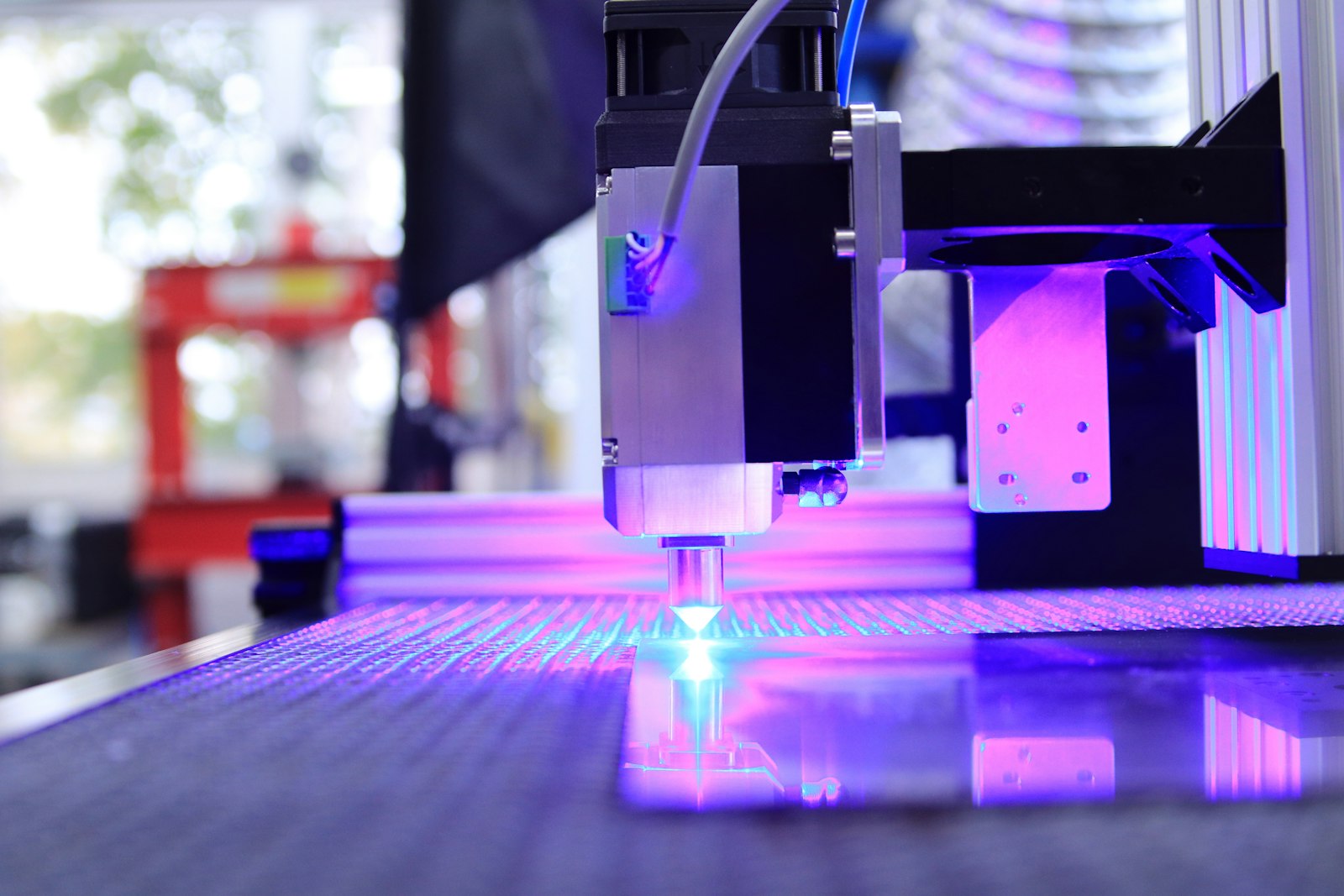
Ultrafast (Femtosecond)
Minimal heat-affected zone
Cold ablation with minimal heat-affected zone, ideal for glass, sapphire, polymers, and thin metal foils where thermal damage or microcracking is unacceptable.
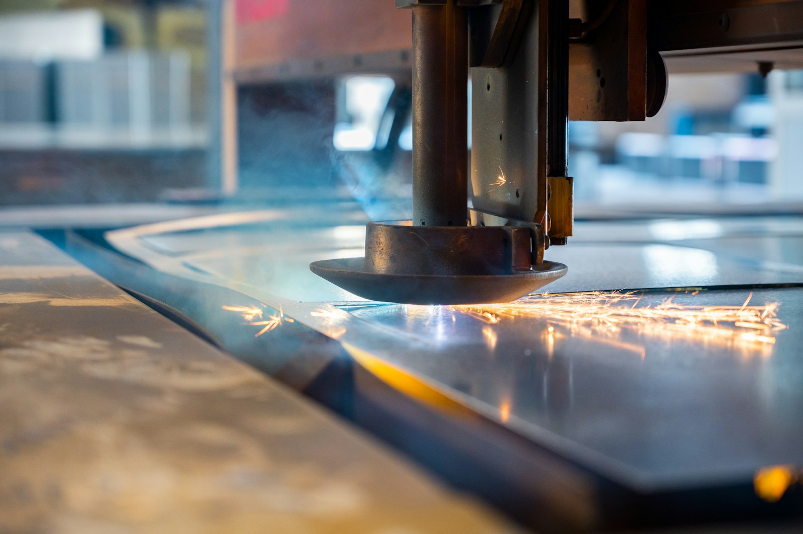
UV (Nanosecond)
Fine kerf, low subsurface damage
High photon energy for clean ablation of polymers, solder mask, and thin-film metallization with fine kerf width and low subsurface damage.
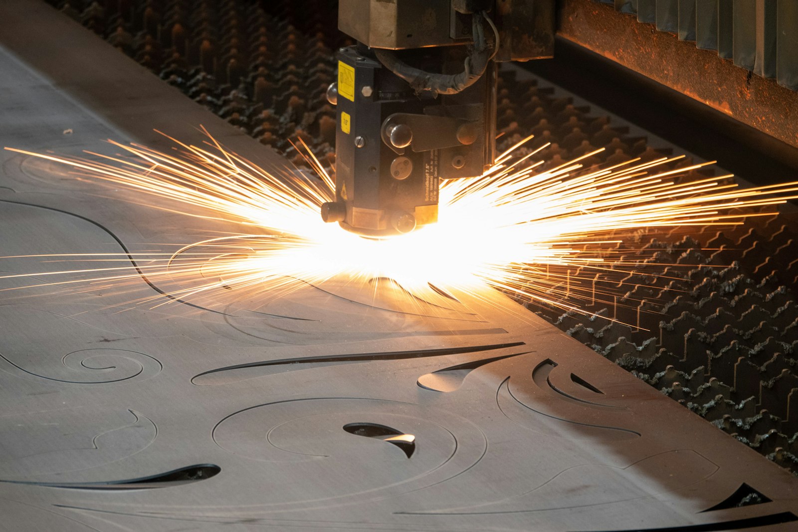
IR / Green (Nanosecond)
Higher throughput
Higher throughput processing for metals and ceramics where feature tolerance is looser and material removal rate matters more than heat-affected zone.
Reference Processing Envelope
Applications
Where Teams Use This Process
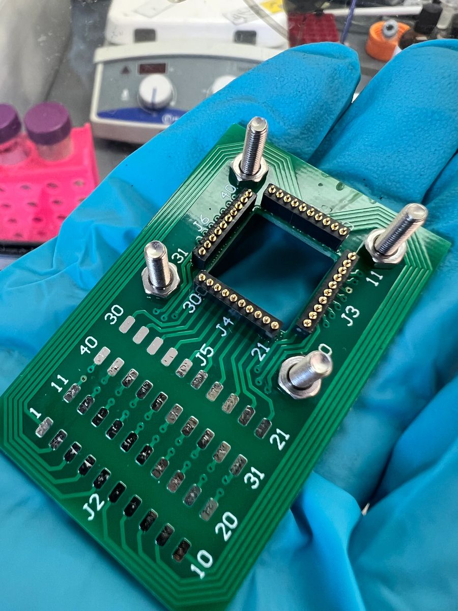
Micro-Drilling & Vias
Fine-feature via formation in flex circuits, MEMS caps, and multilayer ceramic substrates.

Thin-Film Patterning
Selective ablation of ITO, metallization, and dielectric stacks without damaging underlying layers.

Surface Texturing & Marking
Functional micro-texturing for wettability, adhesion, or tribological control, plus permanent traceability marking.

Prototype-to-Production
Process-window development on production-representative material, staged for handoff to your manufacturing partner.
Printed Conductor Trim
Laser definition and trimming of fine-pitch silver/gold ink traces after printing and cure.

Failure Analysis Sectioning
Precision cross-sectioning and cavity access for inspection without mechanical damage to adjacent structures.
Structuring Printed Conductors, Too?
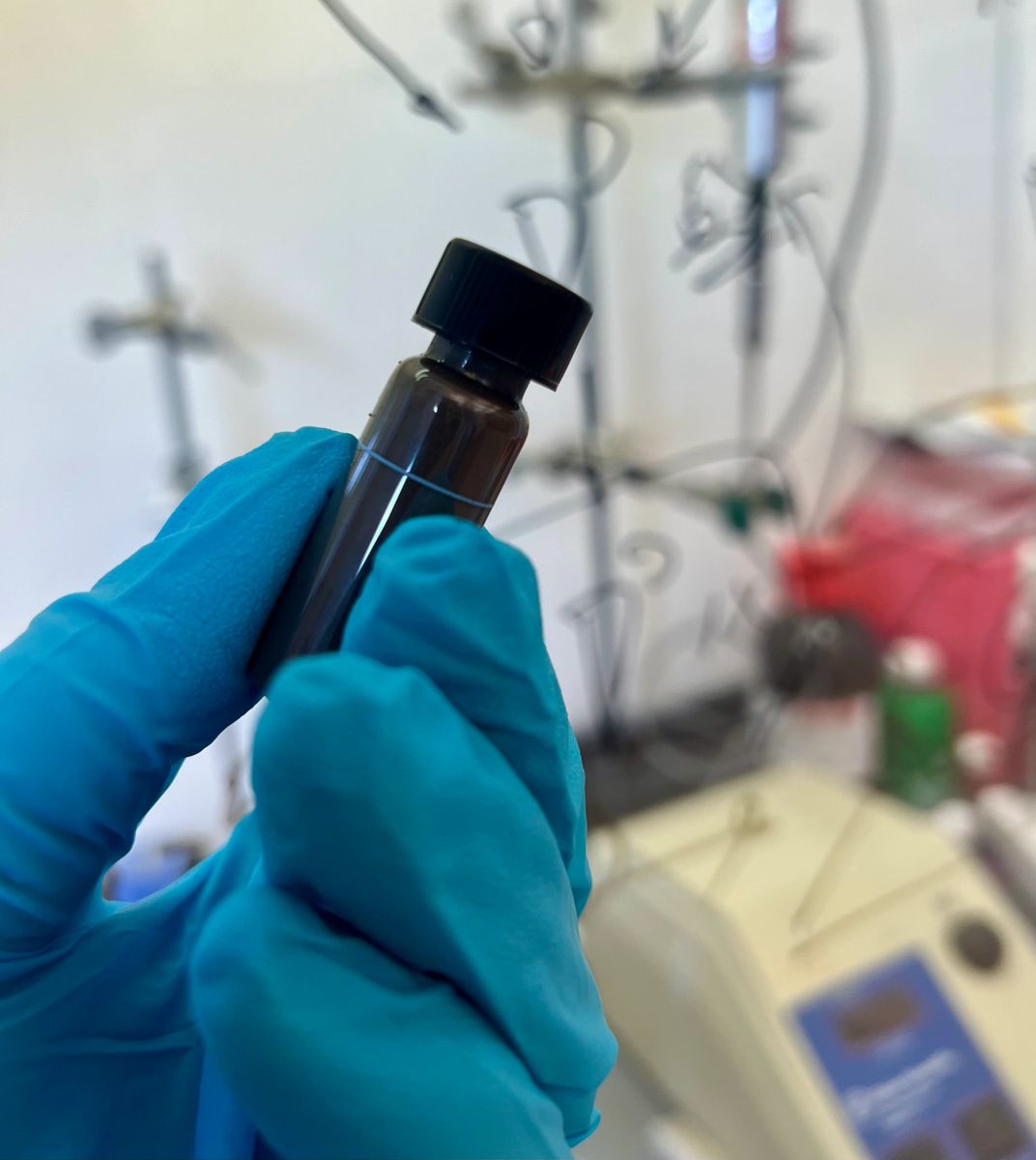
Neuroink formulates electroconductive silver and gold nanoparticle inks for printed electronics. We frequently pair laser structuring with our own printed traces, trimming, singulating, or fine-pitch patterning conductive features after deposition and cure.
FAQ
Laser Micromachining: Common Questions
Why is my laser-drilled via cracking or showing recast?
Longer-pulse (nanosecond) lasers and a wavelength mismatched to your material's absorption profile often leave a heat-affected zone that cracks or recasts material back into the feature. Ultrafast femtosecond ablation removes material faster than heat can diffuse into the surrounding part, minimizing HAZ and recast on glass, sapphire, polymers, and thin metal foils.
Why does my process keep damaging material next to the feature I'm cutting?
That's usually a sign the pulse regime or wavelength is mismatched to your material's absorption profile. We match pulse duration (fs to ns) and wavelength (UV to IR) to the specific material so we remove only the intended feature, not the surrounding structure.
How do you choose between femtosecond and nanosecond processing?
It comes down to your tolerance for heat-affected zone and recast versus throughput needs. We run a short process-window study on your actual material to make this call with data, not a rule of thumb.
Can you match a process developed elsewhere?
Often, yes. Send us the target spec (feature size, tolerance, material stack) and a reference sample if available. We'll characterize the gap and propose a process window, verifying with our profilometry capability where useful.
What volumes do you support?
Engagements typically start with feasibility on a handful of parts, move to a validated process window, and, where it fits your program, scale to pilot-run quantities before handoff to a production partner.
Do you provide process documentation for transfer?
Yes. Every process window is documented with laser parameters, fixturing, and inspection criteria so it can be transferred to your manufacturing or contract partner without re-deriving it from scratch.
Scope Your Next Project
Answer a few questions and we'll route you to a quote, a live demo, or the right spec sheet. No account, no sales gate.

A structured intake form that routes directly to our applications engineers. No account required.